← Network Plug Wiring Diagram Cat 6: Speed Up Your Internet! Cat 6 cable diagram : wiring diagram for cat6 connectors collection Sunroof Wiring Diagram: Fix Electrical Issues Fast! [diagram] bmw x3 sunroof wiring diagrams →
If you are looking for Some LVDS PCB Layout Guidelines for Ensuring Signal Integrity | PCB you've visit to the right place. We have 25 Pictures about Some LVDS PCB Layout Guidelines for Ensuring Signal Integrity | PCB like Practical Guidelines for High-Speed PCB Layout and Critical Component, Some LVDS PCB Layout Guidelines For Ensuring Signal, 40% OFF and also Some LVDS PCB Layout Guidelines for Ensuring Signal Integrity | PCB. Here you go:
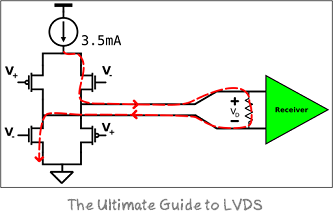
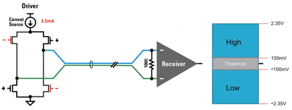
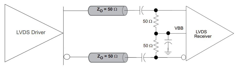
Some LVDS PCB Layout Guidelines For Ensuring Signal Integrity | PCB
 resources.altium.com
Some LVDS PCB Layout Guidelines for Ensuring Signal Integrity | PCB ...
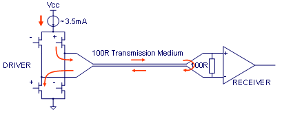
(PDF) AN11088 PTN3460 DP To LVDS PCB Layout Guidelines - DOKUMEN.TIPS
 dokumen.tips
(PDF) AN11088 PTN3460 DP to LVDS PCB layout guidelines - DOKUMEN.TIPS
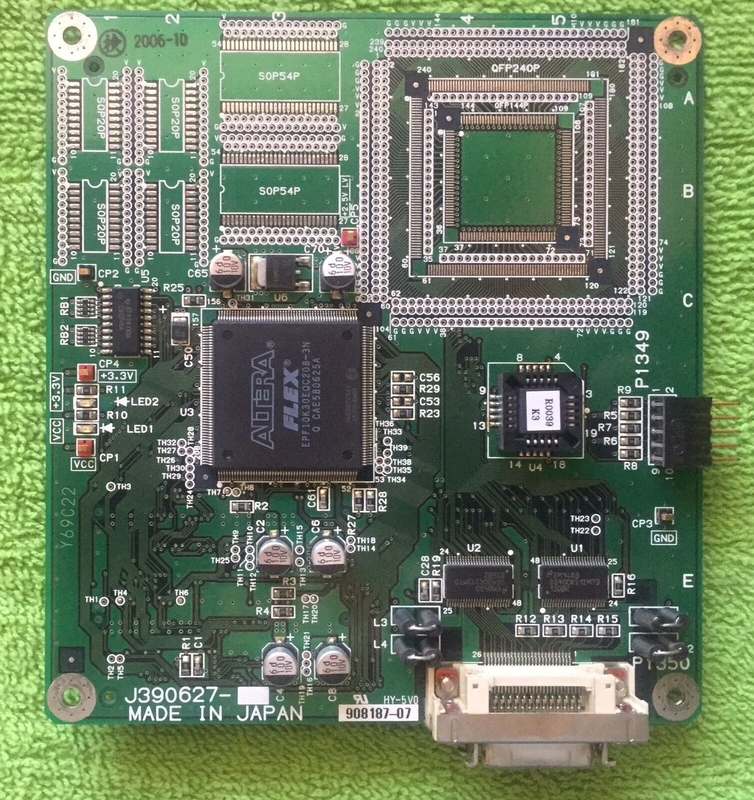
Altera's LVDS System PCB Board Design CloningPCB Reverse Engineering
 www.circuitengineer.com
Altera's LVDS System PCB Board Design CloningPCB Reverse Engineering ...
Some LVDS PCB Layout Guidelines For Ensuring Signal, 40% OFF
 www.oceanproperty.co.th
Some LVDS PCB Layout Guidelines For Ensuring Signal, 40% OFF
Some LVDS PCB Layout Guidelines For Ensuring Signal, 40% OFF
 www.oceanproperty.co.th
Some LVDS PCB Layout Guidelines For Ensuring Signal, 40% OFF
PADS Standard Layout - Mentor Graphics
 www.pads.com
PADS Standard Layout - Mentor Graphics
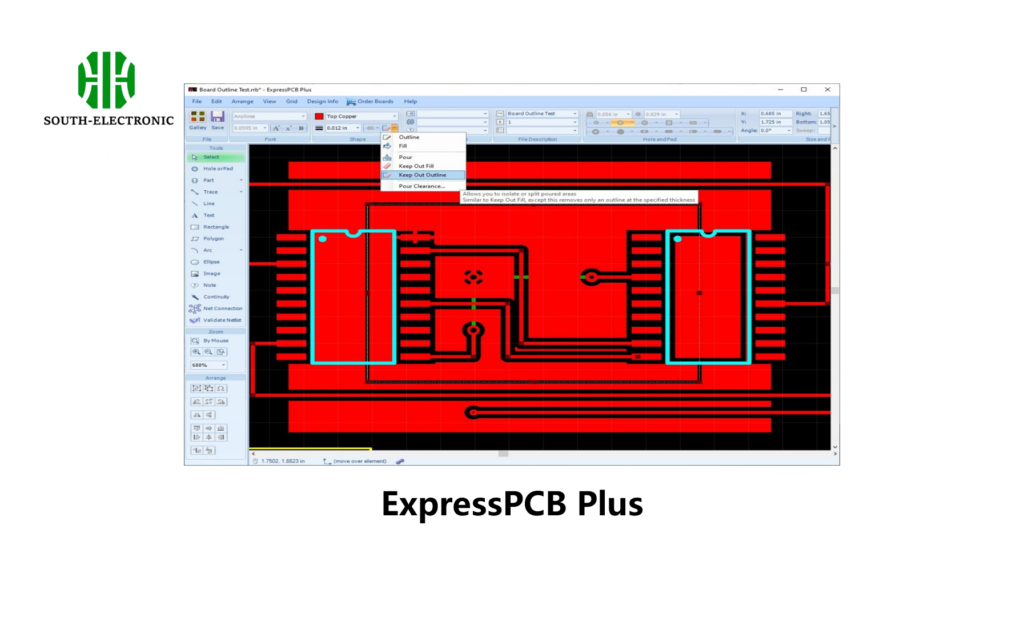
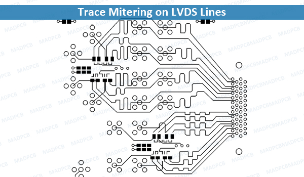
The 13 Most Used PCB Layout Design Tools
 southelectronicpcb.com
The 13 Most Used PCB Layout Design Tools
Some Lvds Pcb Layout Guidelines For Ensuring Signal I - Vrogue.co
 www.vrogue.co
Some Lvds Pcb Layout Guidelines For Ensuring Signal I - vrogue.co
Some LVDS PCB Layout Guidelines For Ensuring Signal Integrity | PCB
 resources.altium.com
Some LVDS PCB Layout Guidelines for Ensuring Signal Integrity | PCB ...
PCB Layout Guidelines For High Speed Applications
 www.linkedin.com
PCB Layout Guidelines For High Speed Applications
Some LVDS PCB Layout Guidelines For Ensuring Signal, 40% OFF
 www.oceanproperty.co.th
Some LVDS PCB Layout Guidelines For Ensuring Signal, 40% OFF
Pcb Layout Guidelines For Design By PCBCART - Issuu
 issuu.com
Pcb layout guidelines for design by PCBCART - Issuu
Pcb Layout Guidelines
 www.wellpcb.com
pcb layout guidelines
Practical Guidelines For High-Speed PCB Layout And Critical Component
 www.scribd.com
Practical Guidelines for High-Speed PCB Layout and Critical Component ...
PCB Layout Services – Electronics Engineering Design Services
 www.microelectronicos.net
PCB Layout Services – Electronics Engineering Design Services
BASIC PCB Design Rules – Layout
 epci.eu
BASIC PCB Design Rules – Layout
Some LVDS PCB Layout Guidelines For Ensuring Signal Integrity | PCB
Some LVDS PCB Layout Guidelines for Ensuring Signal Integrity | PCB ...
Top 5 PCB Design Rules You Need To Know | PCB Design Blog | Altium
 resources.altium.com
Top 5 PCB Design Rules You Need to Know | PCB Design Blog | Altium
Top PCB Design Guidelines Every PCB Designer Needs To Know | Altium
 www.pinterest.co.uk
Top PCB Design Guidelines Every PCB Designer Needs to Know | Altium ...
Some Lvds Pcb Layout Guidelines For Ensuring Signal I - Vrogue.co
 www.vrogue.co
Some Lvds Pcb Layout Guidelines For Ensuring Signal I - vrogue.co
Layout PCB Inverter: Tips And Best Practices For Successful Design
 hillmancurtis.com
Layout PCB Inverter: Tips and Best Practices for Successful Design ...
PCB Design Layout Guidelines For Engineers | Advanced PCB Design Blog
 resources.pcb.cadence.com
PCB Design Layout Guidelines for Engineers | Advanced PCB Design Blog ...
PCB Layout Design By Siemens | PADS Professional | Cadlog
 www.cadlog.com
PCB Layout Design by Siemens | PADS Professional | Cadlog
Practical PCB Design Layout Rules - Leading PCB Manufacturer - Arisentec®
 arisentecpcb.com
Practical PCB design layout rules - Leading PCB Manufacturer - Arisentec®
Practical PCB Layout Tips Every Designer Needs To Know
 www.scribd.com
Practical PCB Layout Tips Every Designer Needs to Know
Pads standard layout. (pdf) an11088 ptn3460 dp to lvds pcb layout guidelines. Pcb layout guidelines for high speed applications